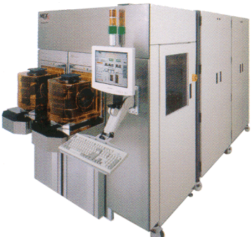
Electro-deposition of metal layers for wafer bumping, redistribution, integrated passives and MEMS.
-Process Applications : Pb Solder, Cu bumps, Cu lines, Cu Via Fill , SnAg Bump, Au Bumps
Patented technology breakthrough “After 20 years of development IBM, you are the first to take vertical wafer plating into production.” Designed specifically for advanced packaging, thick metal deposition Process superiority: better yield on difficult applications Flexibility scalable capacity quick wafer size change ease of chemistry change Lowest cost of ownership
Startus

Description
Product Inquiry
Purchase Product Catalog
Payment & Shipping Conditions:
- Payment: We accept payment through Paypal Only.
- Shipping: We will ship the catalog once the payment is received. And you will be receiving the catalog with in 10 -14 busines days. Shipping might be delayed in due to international shipping conditions which is depends on the countries receiveing. In case hard copy of catalog is not available then we will ship the soft copy.
- Refund: We can refund the order before shipping process was initiated. Incase Catalog not available, we will make sure to refund the order.
- Note: This is a Catalog Produt.
Share Startus in Social Media