Genitech's CMP technology is licensed to Semicontech Corporation.
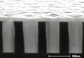
The patterns on ever shrinking semiconductor chips are now as fine as 0.18 micrometer and will go finer. Completely flat surfaces are needed to form such find patterns by lithography. Chemical mechanical planarization (CMP) is used to prepare flat surfaces on wafer. Genitech's unique mechanism, for which patents are pending, provides ideal motion of a polishing pad relative to a wafer. To every point of wafer surface, the pad appears to move in the same way with the same velocity in every direction. Also the displacement of wafer and pad is not large and the motion is mechanically stable.
Advantages
Excellent uniformity
Superior mechanical stability
Small foot-print
Applications
Oxide planarization
Metal planarization
Wafer reclaiming
UNPLA CMP

Description
Product Inquiry
Purchase Product Catalog
Payment & Shipping Conditions:
- Payment: We accept payment through Paypal Only.
- Shipping: We will ship the catalog once the payment is received. And you will be receiving the catalog with in 10 -14 busines days. Shipping might be delayed in due to international shipping conditions which is depends on the countries receiveing. In case hard copy of catalog is not available then we will ship the soft copy.
- Refund: We can refund the order before shipping process was initiated. Incase Catalog not available, we will make sure to refund the order.
- Note: This is a Catalog Produt.
Share UNPLA CMP in Social Media